1 or 0 respectively. Humans prefer expressive, high-level languages. To bridge that gap we use tools:
- A compiler translates high-level code (C, Rust, Go, etc.) into machine code.
- An assembler converts human-readable assembly into machine code.
- The control unit orchestrates the processor: it fetches instructions and signals which parts should act.
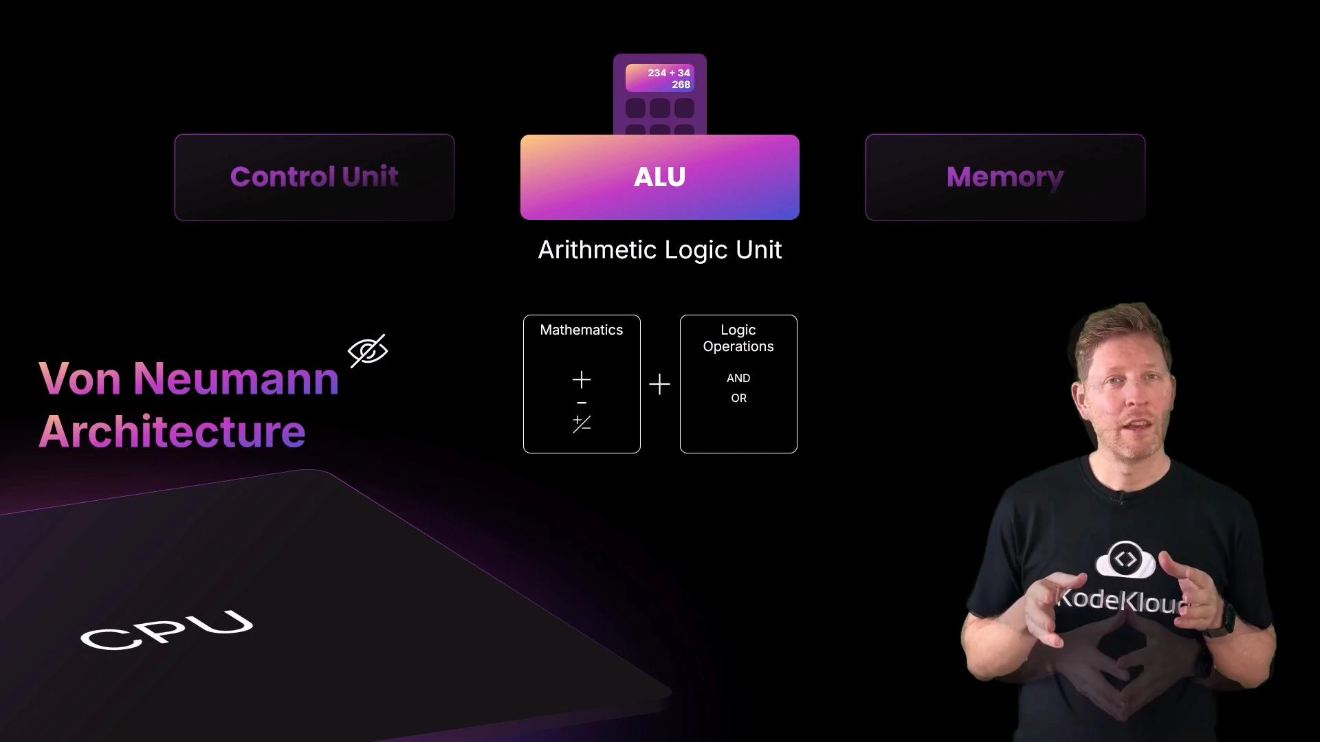
- The ALU performs arithmetic (addition, subtraction, increment) and logic operations (AND, OR, comparisons).
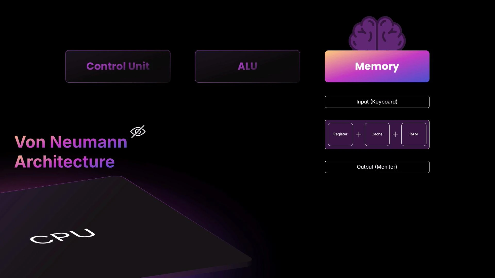
- Memory holds both instructions and data across multiple levels: registers (smallest, fastest), caches (L1/L2/L3), and RAM (larger, slower).
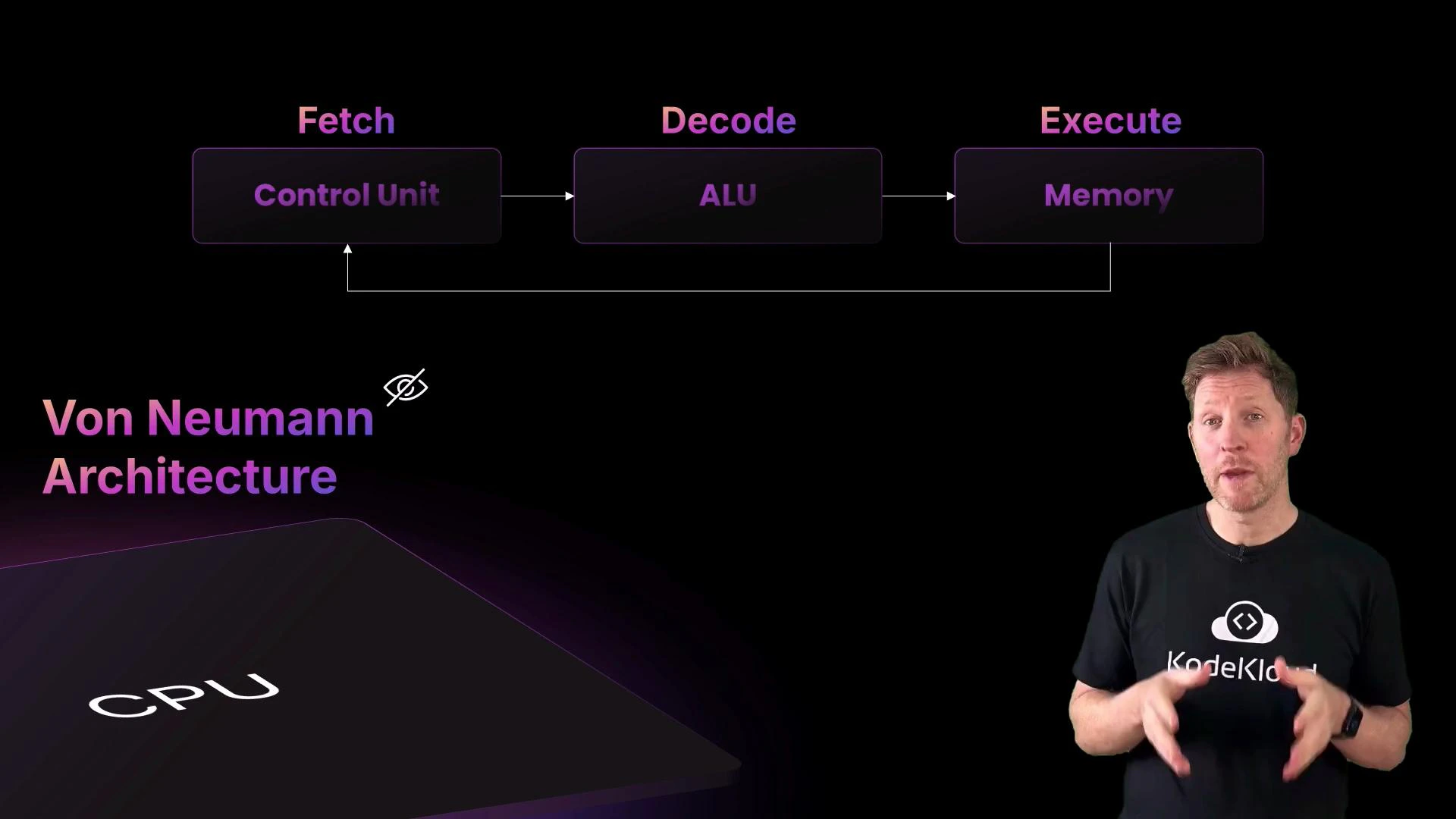
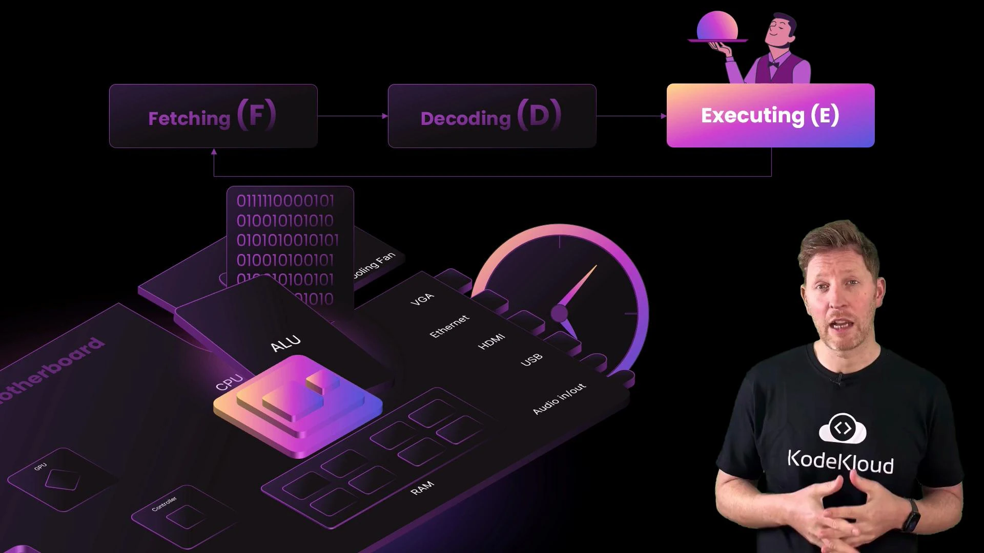
- Fetch: read the next instruction from memory (often from cache) using the program counter (PC).
- Decode: interpret the instruction bits to determine the operation and which operands (registers or memory) to use.
- Execute: perform the operation in the ALU or other execution units, then write results back to registers or memory.
- Customer places an order → user input.
- Fetch: the server (control unit) takes the order to the counter (memory).
- Decode: the server reads the order and tells the chef (ALU) what to prepare; the chef gathers ingredients (data) from the pantry (RAM) to the worktop (registers/cache).
- Execute: the chef prepares the dish (performs computation), places it on the counter (writes result back to memory/register), and the server delivers it to the customer (output).
2 + 2.
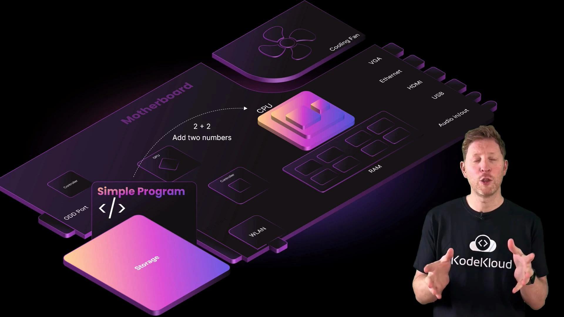
2 + 2:
- The program binary is stored on disk. When launched, the OS loads it into RAM for faster access.
- The FDE cycle begins, driven by the CPU clock:
- Fetch: the control unit fetches the next instruction (e.g.,
ADD R1, R2, R3) from memory using the program counter, placing it into the instruction register. - Decode: the control unit decodes the bits, determining it is an
ADDoperation and where the operandsR2andR3are located. - Execute: the ALU adds the values (for
2 + 2) loaded into registers and writes the result (4) into the destination register or back to memory.
- Fetch: the control unit fetches the next instruction (e.g.,
- The result may then be used by subsequent instructions or sent to an output device (display).
- Increased power consumption
- More heat generation
- The need for better cooling
- Potential instability if thermal, electrical, or timing limits are exceeded
Overclocking can permanently damage hardware and void warranties. Ensure adequate cooling and stability testing before attempting higher clock speeds.
| Concept | Role / Explanation | Example / Note |
|---|---|---|
| Control Unit | Orchestrates instruction flow (fetch & decode) | Manages program counter and instruction register |
| ALU (Arithmetic Logic Unit) | Performs arithmetic and logic operations | ADD, SUB, AND, OR, comparisons |
| Memory Hierarchy | Registers → Cache (L1/L2/L3) → RAM → Storage | Faster, smaller to slower, larger |
| Machine Code | Binary instructions the CPU executes | Produced by compilers/assemblers |
| Clock Speed | Number of cycles per second (GHz) | Higher => faster but more heat |
| Cores & Threads | Parallel execution units | Multi-core CPUs run multiple tasks concurrently |
Tip: To learn more about the von Neumann model and modern CPU optimizations (pipelines, caches, and out-of-order execution), see the Von Neumann architecture and CPU caching resources.
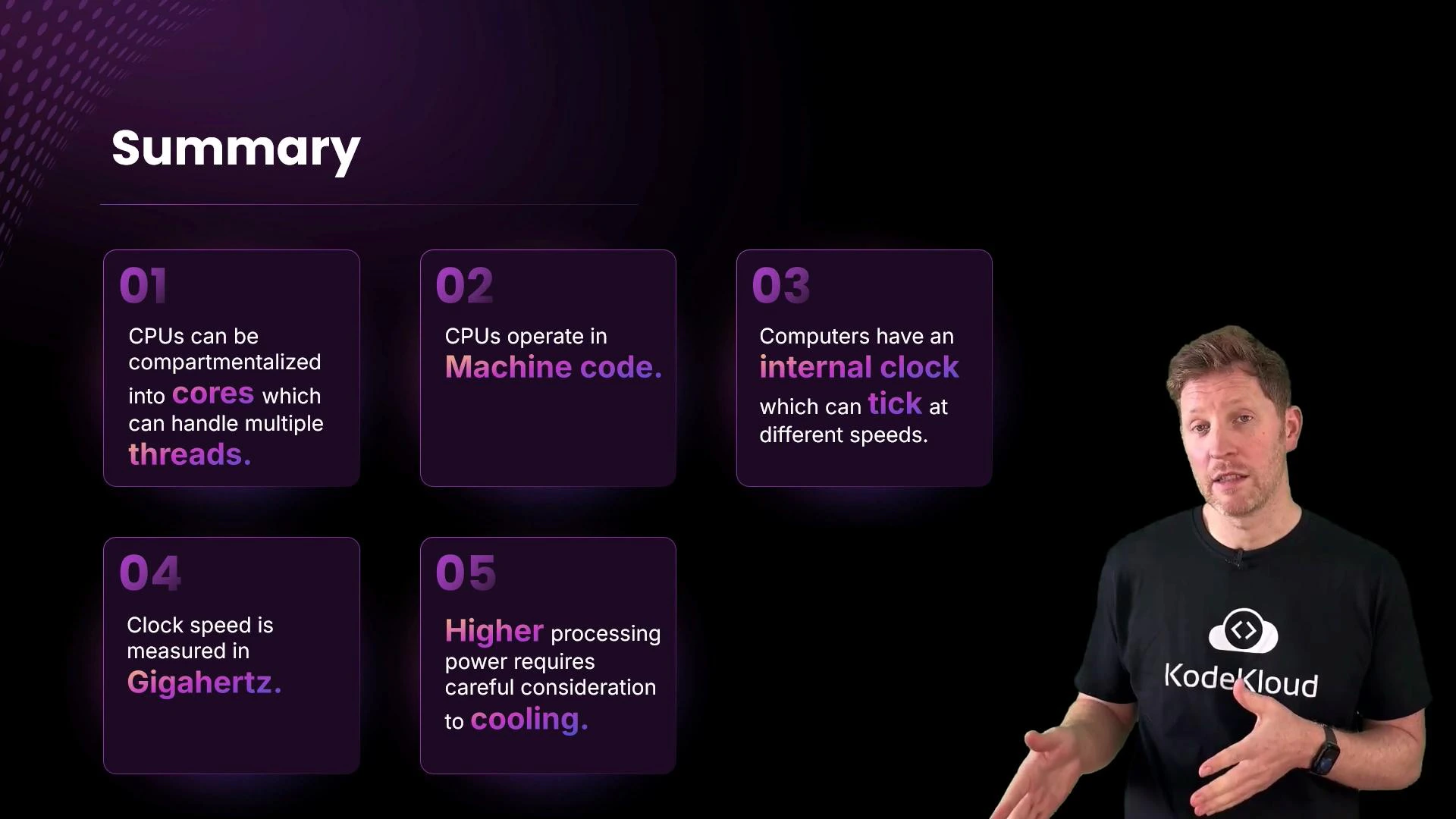
- Modern CPUs are built from billions of transistors that implement binary logic.
- CPUs execute machine code produced by compilers and assemblers.
- The fetch–decode–execute cycle (FDE) is the fundamental loop that runs on every core.
- The CPU clock determines the pace of execution; higher clock speeds increase throughput but also increase heat and power use.
- Multi-core CPUs and threading enable parallel execution for better performance.
- Von Neumann architecture — Wikipedia
- CPU cache — Wikipedia
- Compiler — Wikipedia
- Assembler — Wikipedia